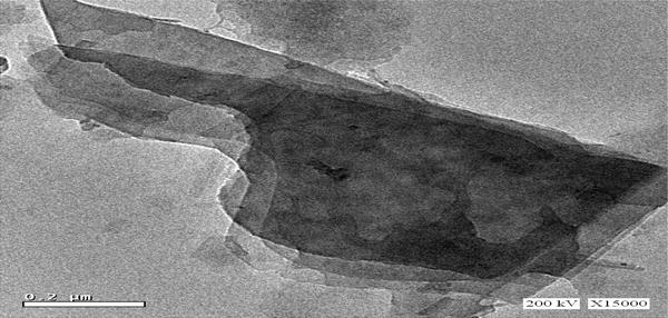
NYCU and TSMC researchers grew an epitaxial interface layer on monolayer MoS2 and reached 0.45 mS per micrometre of transconductance at a 100-nanometre channel.
Silicon transistors are running into a geometric problem. As channels shorten, the gate loses control of the current flowing through them, and the standard remedy — make the conducting body thinner so the gate’s field dominates — eventually asks for a body thinner than silicon can usefully be made.
This is why two-dimensional semiconductors keep appearing in long-range industry roadmaps. A monolayer of molybdenum disulfide is about three atoms thick by construction, with no surface roughness to scatter carriers, which is the geometry a short-channel transistor wants.
A paper in Nature Electronics from National Yang Ming Chiao Tung University, working with TSMC Corporate Research, addresses the step that has held the approach back — and it is not the semiconductor.
The problem is the interface
“Efforts to improve atomically thin transistors have largely focused on discovering better semiconductor materials,” said Professor Wen-Hao Chang of NYCU, a corresponding author. “Our research shows that the atomic interface between materials can be just as important.”
The specific difficulty is depositing a gate insulator onto MoS2. Silicon’s great advantage has always been that it grows its own oxide, a chemically clean insulator bonded directly to the channel. MoS2 has no such oxide, and worse, its pristine surface has no dangling bonds — the chemically reactive sites that atomic layer deposition relies on to nucleate a film.
The result is that high-κ dielectrics deposited on clean MoS2 tend to form islands rather than a continuous layer, leaking where they are thin. The usual workarounds damage the monolayer they sit on, and the damage shows up as charge traps: current that depends on what the device was doing a moment ago rather than on the gate voltage now.
Aluminium, oxidised in place
The method here is to build the interface deliberately. The team deposited an ultrathin epitaxial aluminium layer on monolayer MoS2, then oxidised it to form roughly 0.42 nanometres of aluminium oxide, and grew a hafnium oxide high-κ dielectric on top of that.
Two words carry the weight. Epitaxial means the aluminium was grown with its atomic arrangement registered to the layer beneath rather than deposited as a disordered film, which is what gives the subsequent oxide a smooth and uniform base. And oxidised in place means the oxygen was introduced to a metal already sitting on the monolayer, rather than oxidising species being driven at the MoS2 itself.
The resulting layer does two jobs: a smooth foundation on which the hafnium oxide can grow uniformly, and a buffer that reduces electrical interference between the dielectric and the semiconductor.
At 0.42 nanometres it is roughly one or two atomic layers thick — thin enough that it costs almost nothing in gate control while still separating the two materials.
The numbers
The devices were short-channel top-gate transistors built on CVD-grown monolayer MoS2, with an equivalent oxide thickness near 1 nanometre. They showed low leakage current and minimal hysteresis, and reached a maximum transconductance of 0.45 millisiemens per micrometre at a channel length of about 100 nanometres.
Each of those is a meaningful figure. Equivalent oxide thickness near 1 nanometre means the stack is electrically as thin as a 1-nanometre layer of silicon dioxide, which is the range production logic operates in — a 2D device with a thick gate stack is a laboratory curiosity rather than a candidate. Minimal hysteresis is the direct evidence that the interface is not full of traps, and it is the claim the whole approach rests on. Transconductance measures how much drain current a change in gate voltage buys, which is what determines switching speed and gain.
“When transistor components become only a few atomic layers thick,” said Professor Tsung-En Lee, the other corresponding author, the interface “becomes an active part of the device”. “Learning to engineer these interfaces with atomic precision opens new opportunities,” he said, with Chang adding that the approach let the team “reduce one of the fundamental trade-offs” in these devices.
Why CVD matters more than the transconductance
The detail most relevant to whether any of this leaves the laboratory is the starting material. The monolayers were grown by chemical vapour deposition rather than mechanically exfoliated from a crystal.
A great deal of 2D electronics has been demonstrated on exfoliated flakes — peeled from bulk crystals with adhesive tape, tens of micrometres across, of exceptional quality and no manufacturing relevance whatsoever. CVD growth is scalable and produces films with grain boundaries, defects and thickness variation that exfoliated flakes do not have. A process that works on CVD material is addressing the material a factory would actually use, and the authors’ claim that the work moves closer to wafer-scale manufacturing rests on this rather than on the device metrics.
The distance remaining
Several things a manufacturer would ask are not in the release.
The transconductance is reported as a maximum, which is a best-device number. What determines whether a technology is viable is the distribution across a wafer — the device-to-device variation, the yield, the threshold voltage spread — and the release gives no uniformity statistics at all. Interface engineering is precisely the kind of process whose difficulty is reproducing it identically a billion times.
There is also no comparison with silicon at an equivalent node, which is the benchmark that matters, and no mention of contact resistance. Getting current into and out of a monolayer through metal contacts is the other long-standing obstacle in 2D electronics, independent of the gate stack, and a device can have an excellent interface and still be limited at its contacts.
The TSMC involvement is worth stating plainly. A foundry’s corporate research arm co-authoring a paper on 2D transistor integration is a reasonable signal that the problem is considered worth solving industrially, and it is also an interested party: the work was done with a company whose business depends on the next generation of transistors existing. Nothing in the result is suspect for that reason, and a reader is entitled to know the collaboration is there.
The paper was published on 31 July 2026. The release does not state funding sources or the full author list, gives no affiliation for Lee, and carries only a boilerplate statement that the authors declare no competing interests unless otherwise stated in the published article.
Notes
- “High-transconductance molybdenum disulfide top-gate transistors using epitaxial interface engineering.” Nature Electronics, 2026. DOI: 10.1038/s41928-026-01672-7. The release does not give the full author list.
- National Yang Ming Chiao Tung University. “Engineering the atomic interface opens a new path for atomically thin transistors.” EurekAlert!, 4 August 2026. https://www.eurekalert.org/news-releases/1138925.
Mahmoud Fathy


Leave a Reply