.jpg)
Kyocera Corporation and the Research Institute of Electrical Communication (RIEC) at Tohoku University have developed a new technology that integrates optical isolators directly onto silicon photonics chips using laser annealing — a method that applies localized heat treatment with a laser. The advance addresses a stubborn manufacturing problem standing between silicon photonics and the mainstream data-center hardware it’s meant to make more efficient.
As generative AI and other data-intensive technologies continue to expand, data centers need to process more information while using less energy. Silicon photonics can help by using light to transmit data efficiently, and it’s especially important for Co-Packaged Optics (CPO), which combine optical and electronic circuits in the same semiconductor package to shorten signal paths, reduce signal loss, and lower power consumption. But in optical circuits, some light reflects back toward the laser source, degrading performance. Optical isolators prevent this by allowing light to travel in only one direction — and as optical circuits become smaller and more integrated, demand has grown for isolators that can be fabricated directly onto silicon photonics chips.
Heating Only What Needs Heating
These isolators typically rely on a crystalline material called magneto-optical garnet, which must be heated to 600°C or higher to work properly. Heating an entire chip to that temperature can damage electrodes, wiring, and other components, so the challenge has been to heat only the magneto-optical garnet without overheating the rest of the chip. Kyocera and Tohoku University’s answer is a monolithic integration technology that uses laser annealing to do exactly that — a laser heats only the areas of the chip that require treatment.
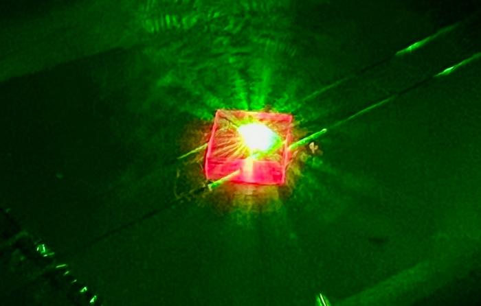
A near-infrared laser beam is applied only to the optical isolator circuit region, which measures about 700 by 700 micrometers and contains a magneto-optical garnet film. The localized heating causes the garnet to crystallize, giving it the properties needed to suppress reflected light, while limiting the heat exposure of surrounding optical circuits and electrodes — unlike conventional methods that heat the entire chip in a furnace.
Using this technology, the research team fabricated a device that uses light interference and experimentally demonstrated its operation as an optical isolator. Comparing the optical output of forward-propagating signal light with that of backward-propagating reflected light, the results confirmed “an isolation ratio of 13.6 dB in the optical communication wavelength range, corresponding to an approximately 95% reduction in back-reflected light.” Electron microscopy also confirmed that the magneto-optical garnet in the laser-irradiated area had successfully crystallized on the silicon waveguide.
Kyocera and Tohoku University have previously collaborated on related optical isolator technologies for optical circuits. To move this one toward commercialization, the two organizations aim to achieve “lower optical loss, higher efficiency, and improved productivity for mass production,” and plan to continue their collaboration toward a more efficient and sustainable information society.
The study, “Monolithic Magneto-Optical Mach-Zehnder Isolator Using Laser-Annealed Iron Garnet on a Silicon Waveguide,” was published in IEEE Access (DOI: 10.1109/ACCESS.2026.3729586).

Leave a Reply