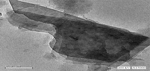

This Transmission Electron Microscopy (TEM) image depicts a graphene sheet, which is a monolayer of carbon atoms arranged in a two-dimensional honeycomb lattice. The sample has been magnified significantly, allowing for a detailed view of its structure. The scale at the bottom left corner shows a 0.2 µm marker, indicating the fine resolution typically achievable in TEM analysis, while the magnification level is marked as 15000x.
Graphene, due to its unique physical and chemical properties, has gained attention in fields such as materials science, nanotechnology, and electronics. In this TEM image, the thin sheet structure is visible, showing the characteristic transparency of graphene at atomic thicknesses. TEM is a particularly powerful tool for visualizing such materials because it allows scientists to examine the crystal structure, defects, and edges of graphene sheets at atomic resolution.
The image shows slightly uneven regions, which may correspond to folds, wrinkles, or variations in the number of graphene layers. Such defects are typical in synthesized graphene samples and can influence the material’s mechanical and electronic properties. Defects like these could lead to changes in conductivity, chemical reactivity, or strength.
The darker regions suggest areas where multiple layers of graphene might have stacked, creating localized thicker zones. Meanwhile, the lighter, more transparent regions likely indicate a monolayer or thinner sections of graphene. These variations in thickness are often a point of interest when evaluating graphene samples because they directly affect its optical, thermal, and conductive behavior.


Leave a Reply